Ultrapure & High-Purity Water Systems for Semiconductor, FPD, OLED & PCB — 18.2 MΩ·cm, SEMI F63 / IPC-9592
Two-pass RO + EDI + mixed-bed polish + 185 nm UV for wafer fabs (18.2 MΩ·cm), and RO → EDI → sub-loop polish for display & PCB cleaning (10–16 MΩ·cm). Built for wafer fabs, advanced packaging, OLED/LCD, and compound-semiconductor lines. Capacities from 0.5 t/h lab pilot to 100 t/h production trains.
Request a UPW Sizing Sheet Talk to a semiconductor engineer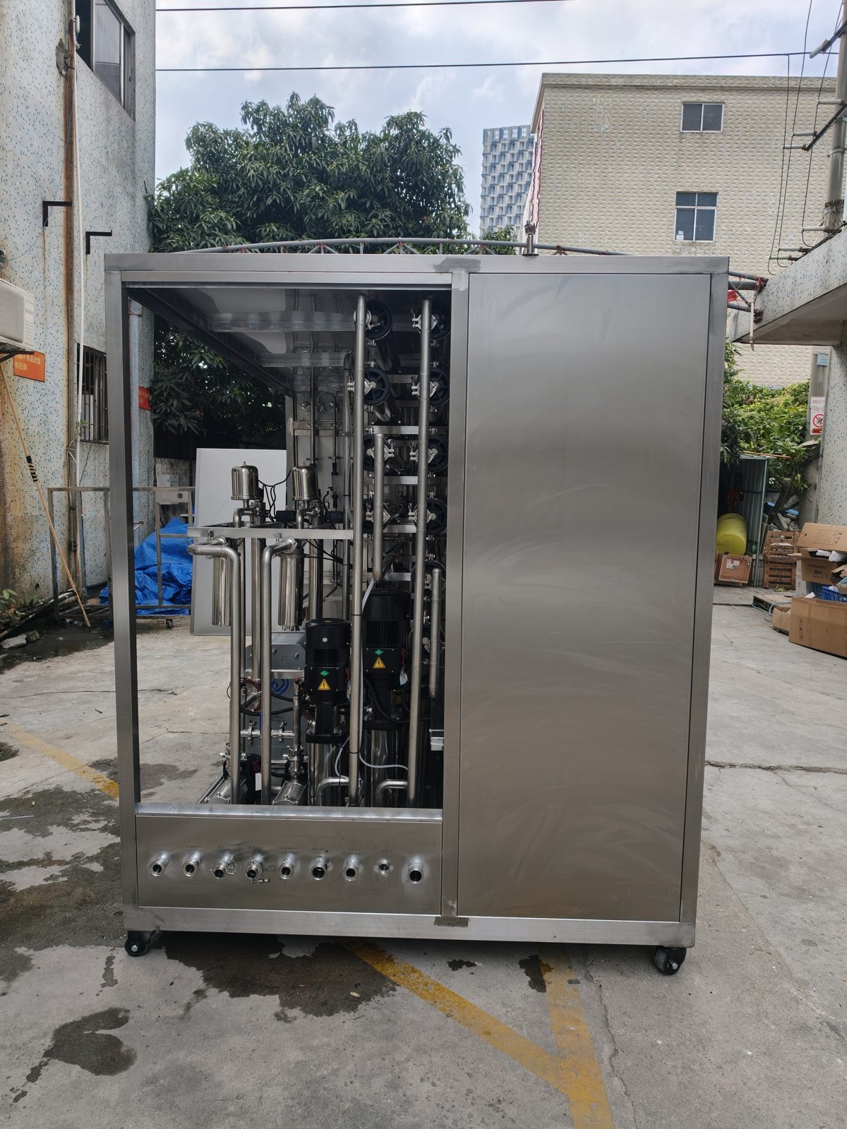
Why Semiconductor Fabs Cannot Tolerate Anything Less Than 18.2 MΩ·cm
A single 0.1 µm particle or 1 ppb TOC excursion can scrap an entire lot of EUV-patterned wafers. We engineer to SEMI F63 and ASTM D5127-13 Type E1.1 / E1.2, sized to hold these numbers during transient demand — not just at steady state.
| What you measure | Why it matters | Target we hold |
|---|---|---|
| Resistivity | Total ionic contamination | 18.2 MΩ·cm @ 25 °C |
| TOC | Photoresist defects | < 5 ppb (online) |
| Particles | Pattern defects | < 1/mL @ ≥ 0.05 µm |
| Silica | Deposits on wafer | < 0.5 ppb |
| Bacteria / endotoxin | Yield killer | < 1 CFU/L |
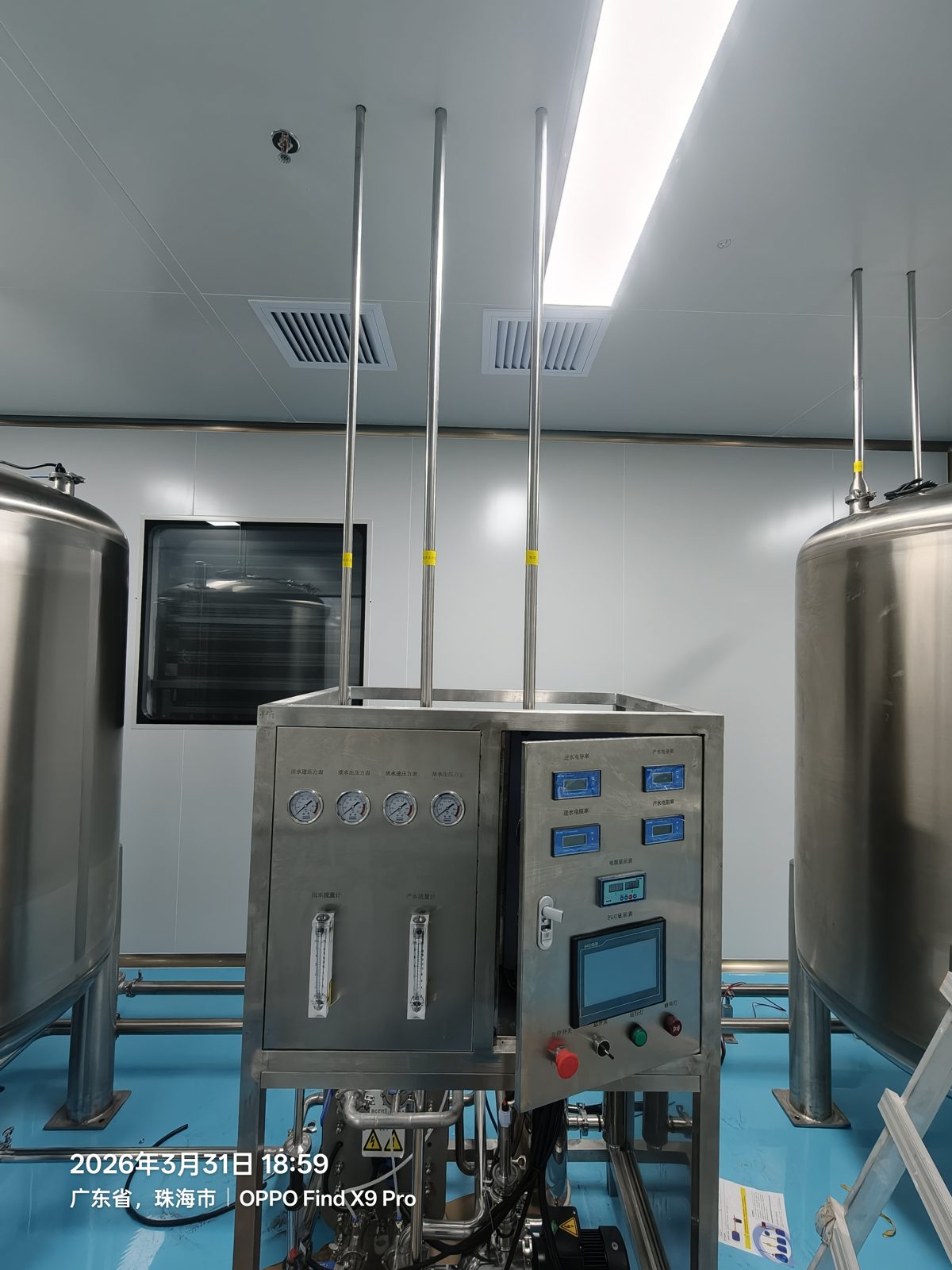
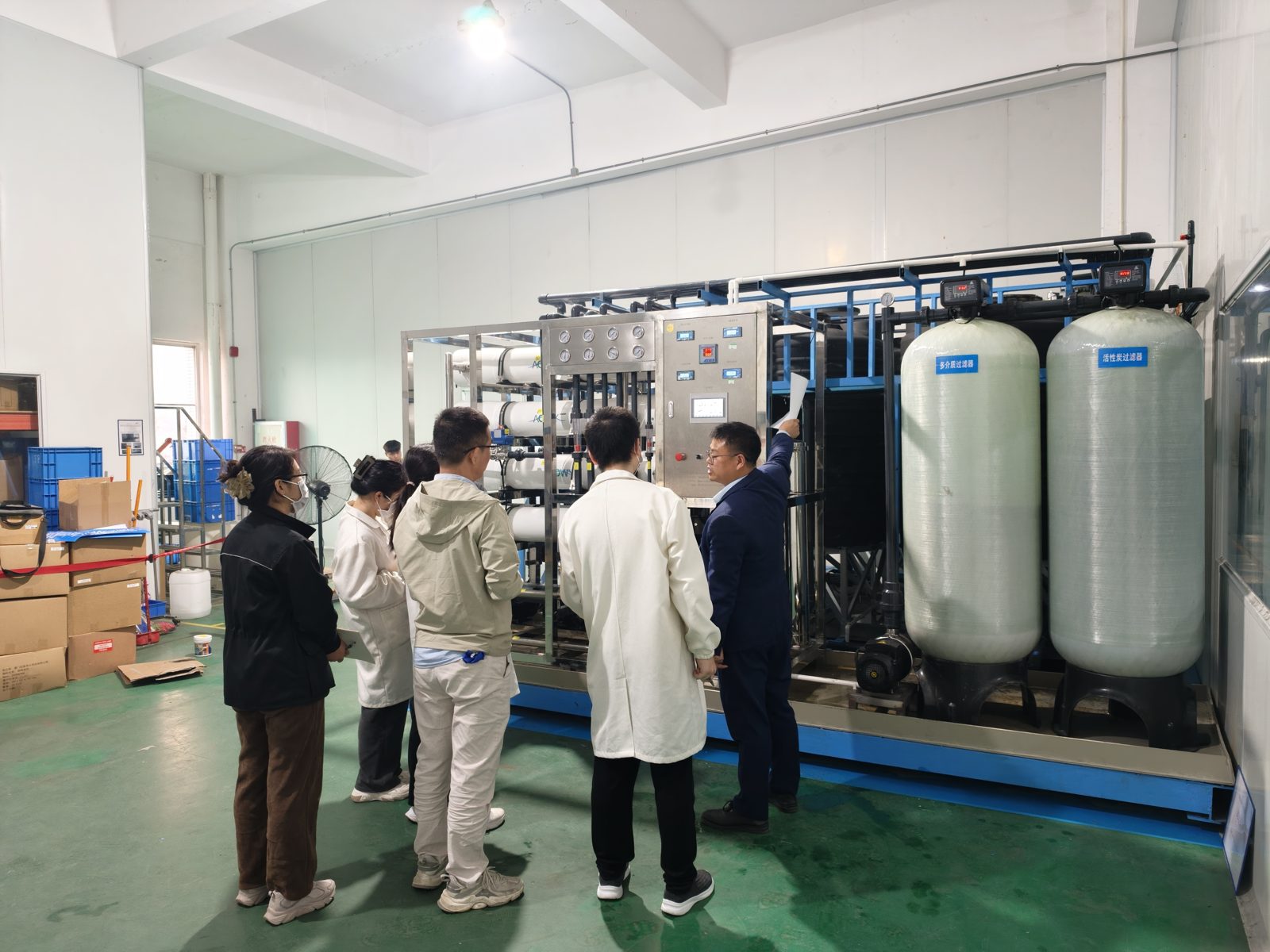
Our Standard UPW Process Train
| Stage | Equipment | Function | Key spec |
|---|---|---|---|
| ③ 1st-pass RO | DOW™ BW30-400 | Remove 95–99% ions | Recovery 75–80% |
| ④ 2nd-pass RO | DOW™ BW30-4040 | Push to < 5 µS/cm | Recovery 90% |
| ⑤ EDI | Veolia / Suez / QKH-EDI | Continuous ion removal | 15–18 MΩ·cm |
| ⑥ Mixed-bed polisher | Nuclear-grade MB | Final polish to 18.2 MΩ·cm | MB life 12–18 months |
| ⑦ 185 nm UV | TOC reduction | Photo-oxidise residual TOC | ≥ 30 mJ/cm² |
| ⑨ Loop | EP 316L SS / PVDF / PFA | Hold resistivity at point-of-use | Ra ≤ 0.8 µm, 1.5–2 m/s |
Overall recovery 85–90%, with reject routed to UPW reclaim and scrubber make-up.
Materials We Use
| Wetted part | Material | Surface finish |
|---|---|---|
| RO vessels | FRP with vinyl ester liner | — |
| Distribution piping | Electropolished 316L SS / PVDF / PFA | Ra ≤ 0.8 µm |
| Tanks | HDPE-lined CS / PP / PVDF | No metal contact |
| Valves | Sanitary diaphragm, EPDM/PTFE | No dead legs |
| Welds | Orbital, argon-purged | Passivation ASTM A967 |
Standard Capacities
| Model | Output | Power | Typical application |
|---|---|---|---|
| UPW-0.5 | 0.5 t/h | 4 kW | R&D / lab pilot |
| UPW-2 | 2 t/h | 12 kW | Pilot line, OLED R&D |
| UPW-5 | 5 t/h | 25 kW | Small-batch fab |
| UPW-10 | 10 t/h | 50 kW | 6"/8" fab |
| UPW-20 | 20 t/h | 95 kW | 8"/12" fab |
| UPW-50 | 50 t/h | 220 kW | 12" advanced fab |
| UPW-100 | Custom | Custom | Mega-fab |
Engineering Reference — 50 t/h UPW for a 12" Wafer Fab
| Parameter | Design value |
|---|---|
| Feed | City water, TDS ≈ 200 ppm, silica ≈ 8 ppm |
| UPW demand | 50 t/h, 1.3× peak factor |
| Loop | 1.8 m/s, 3× tank turnover/h |
| UPW quality | 18.2 MΩ·cm, TOC < 5 ppb, particles < 1/mL |
| RO / EDI | Two-pass 85% recovery; two EDI trains 25 t/h each |
| Distribution | EP 316L SS, Ra ≤ 0.8 µm, PFA-lined final 20 m |
| Controls | Siemens S7-1500, Profinet to fab SCADA, optional SECS/GEM |
| Delivery | 18–22 weeks from PO |
For FPD, OLED & PCB Lines — High-Purity Water, Not Full UPW
Most display and board fabricators do not need 18.2 MΩ·cm. FPD color-filter washing, OLED evaporation-chamber cleaning and PCB rinse/etch lines are correctly spec'd to 10–16 MΩ·cm cleaning water plus a separate, lower-grade process loop. Specifying full UPW where it is not needed costs roughly 30–50% extra capex and 40–60% higher operating cost for no yield gain — we engineer to the right spec for the line.
| What you measure | Why it matters | Target we hold |
|---|---|---|
| Resistivity (cleaning) | Ionic residue on glass / wafer / PCB | 10–16 MΩ·cm @ 25 °C |
| TOC (cleaning) | Streaking on display, hazing on glass | < 50 ppb (online) |
| Particles | Display mura, PCB solder defects | < 10/mL @ ≥ 0.1 µm |
| Silica | Glass staining | < 5 ppb |
| Bacteria | Biofilm in sub-loop | < 10 CFU/L |
| Process loop (etch/CMP) | Recirculated for reclaim | 1–5 MΩ·cm depending on stage |
Most FPD and Gen-6+ OLED lines do not need mixed-bed polishers in the main loop — EDI + 185 nm UV + sub-loop tank holds ~15 MΩ·cm at point-of-use. We add MB polish only when a single demanding tool (e.g. EUV-adjacent metrology) or borderline feed water requires it. Optional UF + RO CMP reclaim skid recovers 60–80% of etch/CMP wastewater back to pretreatment.
Engineering Reference — 10 t/h Cleaning Water for a Gen-6 OLED Line
| Parameter | Design value |
|---|---|
| Feed | City water, TDS ≈ 200 ppm, silica ≈ 8 ppm, free Cl₂ < 0.5 ppm |
| Cleaning demand | 10 t/h avg, 1.4× peak |
| Cleaning water quality | 15 MΩ·cm @ point-of-use, TOC < 30 ppb, particles < 5/mL @ ≥ 0.1 µm |
| Process loop (etch/CMP) | 2 t/h reclaim via UF + RO, returned to feed |
| Sub-loop | PFA-lined final 15 m, 1.8 m/s, 3× tank turnover/h |
| Controls | Siemens S7-1500 / Allen-Bradley CompactLogix, Profinet to fab DCS |
| Delivery | 12–16 weeks from PO |
5 Pitfalls We Design Around
- TOC excursion during EDI start-up — online TOC on EDI outlet; ramp UPW-to-tools only after TOC < 10 ppb for 24 h.
- Particle spikes after MB regeneration — pre-test at FAT; 3-day on-site handover.
- Bacterial growth in the loop — sized ≥ 1.5 m/s with periodic hot sanitisation (≥ 80 °C) and/or ozone.
- Silica breakthrough on EDI — pre-RO pushes silica below 0.5 ppm; checked in pre-engineering.
- MB lifetime wasted on CO₂ absorption — N₂ blanket and HEPA vent filters keep MB life at 12–18 months.
- Over-spec to full UPW when 10–16 MΩ·cm is enough (FPD/OLED/PCB) — we ask for the line's most demanding point-of-use first, then size back. UPW-only quotes on display lines cost buyers 30–50% more for no yield gain.
Standards We Design To
- SEMI F63 — UPW for semiconductor processing
- ASTM D5127-13 — Type E1.1 / E1.2 (wafer UPW) and E2 / E3 (display/PCB cleaning water)
- IPC-9592 — Water quality for PCB manufacturing
- ASTM D5128 — On-line TOC analysis
- ISO 14644-3 — Cleanroom compatibility
- CE / IEC 61010 / IEC 61326
- ISO 9001 / ISO 14001
Frequently Asked Questions
Q1. What resistivity can your UPW system actually hold?
For wafer fabs, 18.2 MΩ·cm at point-of-use, validated at FAT and on-site SAT. For FPD / OLED / PCB cleaning lines we hold 10–16 MΩ·cm — spec'd to the line's real requirement so you are not paying for UPW you do not need. Mixed-bed polisher sized for 12–18 months between regenerations.
Q2. Can you integrate with our fab SCADA / MES?
Yes — Modbus TCP / Profinet / EtherNet/IP standard; optional SECS/GEM (SEMI E30/E84/E87).
Q3. How long does delivery + installation take?
12–14 weeks for ≤ 20 t/h; 18–22 weeks for 50 t/h. On-site installation 3–4 weeks for a 20 t/h skid.
Q4. What feed water do you accept?
Potable city water TDS ≤ 500 ppm. Surface/river/seawater needs a UF pretreatment skid.
Q5. Do you provide IQ/OQ documentation?
Yes — full IQ/OQ/PQ in English, FAT in our factory, SAT at your site, material traceability (3.1 certs) and calibration certificates.
Q6. What is the warranty?
12 months on the whole system + 36 months on critical parts (RO membranes, EDI stacks, UV lamps).
Q7. Do you supply consumables and spares?
Yes — 2-year consumables forecast; standard spares stocked in our Shenzhen warehouse for 7-day international dispatch.
Q8. Can we visit your factory for a FAT?
Yes — customer FATs at our Shenzhen facility, or remote video FAT.
Related Equipment & Industries
RO-4000 — Reverse Osmosis · DI-1000 — Deionized Water · PW-1500 — GMP Purified Water · UF-2000 — Ultrafiltration · WFI-1000 — Water for Injection
Pharmaceutical & Biotech (GMP) · Food & Beverage (process water) · Power Plant (Utility Make-Up)
Ready to Spec Your UPW System?
Get a free sizing sheet + SEMI F63 compliance checklist within 24 h.
Request a UPW Sizing Sheet Talk to a semiconductor engineerTechnical content reviewed by Ella Liu, Industrial Water Treatment Specialist at Rong Water — 10+ years sizing RO, EDI and ultrapure / high-purity water systems for semiconductor, display (FPD/OLED) and electronics clients.